



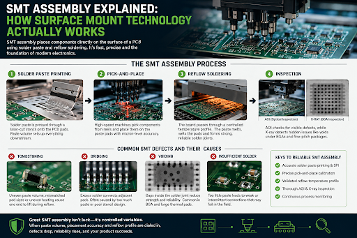
Most if not all PCBs manufactured today use SMT assembly, the acronym covers some physics you didn’t think were included within these few minutes on a factory floor: Solder has to print within micron tolerances at a very specific volume, place component within micron tolerances on a pad, the reflow oven has to ramp the PCB at a very specific temperature profile and do it without tilting component or warping the board. Miss one step, and you get a tombstoned resistor or a bridged BGA. This is what actually happens inside SMT assembly, and why the process is far less forgiving than it looks from the outside.
What Is SMT Assembly?
SMT, or surface mount technology, is the method of soldering electronic components directly onto pads on a PCB’s surface, rather than inserting leads through drilled holes as with through-hole assembly. It is the primary assembly technique for electronic products used today, and with 2026 EMS market data demonstrating that the percentage of all activity involved in the manufacturing services sector carried out based on surface-mount technology approaches and well exceeds one-half of the business the reason should be apparent, the number of components which it is possible to accommodate on the surface of the component mounting base, and ease with which components could be placed at high speeds on automatic machinery.
A surface-mount assembly has four main steps: solder paste printing, component placement, reflow soldering, and inspection. Each step has potential failure points, and knowing them distinguishes a good SMT run from a rework frenzy.
The SMT Assembly Process Step by Step
Solder Paste Printing
A laser-cut stencil sits over the board, and solder paste gets pushed through its openings onto exposed copper pads. Paste volume here sets up nearly everything downstream — industry data puts solder paste printing behind over half of all SMT reflow defects, more than any other single stage in the process.
Pick-and-Place
Fast automated placement machines scoop up the tiny parts from reels with vacuum heads, placing them onto the paste pads, and can produce tens of thousands of insertions per hour. The pressure must be balanced: too little and the component could dislodge during reflow; too much and it can squeeze paste out from under it.
Reflow Soldering
The board travels through an oven following a controlled temperature profile — preheat, soak, reflow, cooling. The paste melts and wets the pads before solidifying to a permanent joint. Lead-free solder is now the norm; it melts at around 217C and provides a less generous margin of error than older, lead-based solder, which is partly why reflow profiling is such an exact science now.
Inspection
Automated optical inspection checks for missing components, misalignment, and visible solder defects after reflow. X-ray inspection picks up what AOI can’t see — voids and hidden joint issues under BGA packages, where the solder connection sits underneath the component itself.
What Causes the Most Common SMT Defects?
Most SMT defects trace back to an imbalance somewhere in paste volume, placement accuracy, or thermal profile — rarely to random chance.
Tombstoning
One end of a small passive component lifts during reflow and stands upright, disconnected on one side. It happens when wetting forces are unequal between the two pads — uneven paste volume, mismatched pad sizes, or uneven heating across the board. Small chip components like 0402s and 0201s are especially prone to it, since there’s so little mass anchoring them down.
Bridging
A “Bridge” forms when excess solder connects to an adjacent pad, which usually happens during the stencil design/solder paste printing process rather than at the component placement stage. The risk becomes very high with fine-pitch components that have very narrow spacing between adjacent pads, which is why stencil aperture design often receives so much focus on very dense board assemblies.
Voiding and Insufficient Solder
Gaps inside a solder joint reduce its thermal and mechanical strength, even when the joint looks fine from the outside — this is exactly why BGA joints need X-ray, not just visual inspection. Insufficient solder produces the opposite problem: too little paste on the pad leaves a weak or incomplete connection that may pass initial testing and fail months later in the field.
Choosing an SMT Assembly Partner That Controls These Variables
None of these defects are inevitable — they’re process signals, and a manufacturer with tight discipline around solder paste inspection (SPI), calibrated pick-and-place equipment, and validated reflow profiles catches them before a board ever reaches AOI. When you’re evaluating an SMT assembly service, ask specifically how they control paste volume at the printing stage and whether they run SPI before placement — that single checkpoint prevents more downstream defects than almost anything else in the line.
Conclusion
While externally, SMT assembly appears automatic and passive, the quality you achieve from the bottom up depends on how well a manufacturer manages paste volume, placement repeatability, and thermal profiling-the same three factors that cause almost any typical SMT defect. If you know why tombstoning, bridging, or voiding occur, you’ll be better prepared to ask the manufacturer questions before signing off on the job.
